
At Precintl, we help product creators, original equipment manufacturers (OEMs), and original design manufacturers (ODMs) turn complex electronic ideas into market-ready physical hardware. This guide breaks down the full electronics lifecycle, offering practical engineering insights to help you build reliable, manufacturable, and cost-effective circuit boards.
Printed circuit boards form the physical and electrical foundation of modern electronics. Every hardware product—from consumer wearables and industrial sensors to automotive control modules—relies on a well-engineered circuit board to route signals, distribute power, and hold electronic components securely in place.
Executing a successful hardware project requires more than drawing schematic lines between component pins. It demands a holistic engineering methodology that bridges concept creation, layout optimization, Design for Manufacturing (DFM), prototype fabrication, surface mount assembly, and volume production. Understanding how to design a PCB while accounting for real-world fabrication tolerances, component availability, and electromagnetic behavior separates functional hardware from costly project delays.
What Is PCB Design?
PCB Design Definition and Purpose
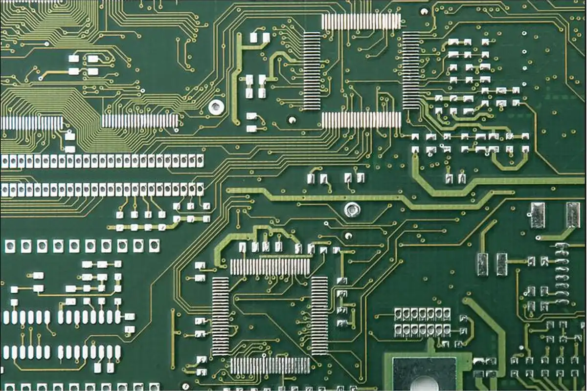
PCB design is the engineering discipline of converting theoretical electronic schematics into physical, multi-layered circuit board layouts. The ultimate purpose of this process is to establish reliable electrical connections between active and passive components while satisfying mechanical enclosures, thermal constraints, and regulatory requirements.
PCB Design vs. PCB Layout: What Is the Difference?
While often used interchangeably, schematic creation and physical placement serve distinct functions:
- PCB Schematic Design: Defines the logical architecture of the circuit. It specifies component symbols, pin numbers, signal nets, and functional relationships without spatial or mechanical representation.
- PCB Layout Design: Translates schematic logic into physical reality. It involves placing actual component footprints, routing copper traces, defining layer stackups, and managing physical spacing constraints on a copper-clad substrate.
Why PCB Design Matters for Product Development and Manufacturing
Poor design choices ripple throughout the entire supply chain. A flawed board layout can introduce signal distortion, cause thermal overheating, fail electromagnetic compatibility testing, or prove impossible to assemble efficiently on automated machinery. Investing time in disciplined layout decisions directly reduces engineering change orders (ECOs), shortens product development cycles, and lowers overall manufacturing costs.
What Are the Main Types of PCB Design?
Different applications require specific board constructions to balance mechanical flexibility, signal speed, thermal performance, and unit cost.
| PCB Type | Description |
|---|---|
| Single / Double Layer | Low cost, basic consumer goods |
| Multilayer (4-32+) | High density, tight signal routing |
| Flexible & Rigid-Flex | Dynamic bending, tight enclosures |
| High-Speed / High-Density | Controlled impedance, microvias, HDI |
Single-Layer PCB Design
Single-layer designs utilize a single copper laminate layer bonded to a dielectric substrate. They represent the simplest, lowest-cost fabrication option, commonly found in high-volume, basic consumer electronics such as power supplies, LED lighting, and simple household appliances.
Double-Layer PCB Design
Double-layer boards feature copper traces on both top and bottom surfaces, connected through plated through-holes (vias). This structure provides significantly more routing flexibility, allowing engineers to dedicate one layer to signal routing and the other to ground or power distribution.
Multilayer PCB Design
Multilayer PCB design incorporates four or more conductive copper layers separated by internal dielectric prepreg and core materials. Multilayer architectures enable complex signal routing, dedicated ground and power planes, controlled impedance traces, and enhanced noise immunity. High-density consumer devices and commercial compute modules routinely use 6, 8, 12, or more layers.
Flexible and Rigid-Flex PCB Design
Flexible PCBs use polyimide substrates instead of traditional FR-4 glass-reinforced epoxy. They bend and flex inside tight enclosures, eliminating bulky wire harnesses. Rigid-flex boards merge flexible ribbon sections with rigid multilayer sections, delivering robust mechanical durability for aerospace, medical, and high-reliability wearable devices.
High-Speed and High-Density PCB Design
High speed PCB design deals with signals operating at frequencies where trace length, board dielectric constants, and parasitic inductance directly impact signal integrity. High-Density Interconnect (HDI) boards utilize microvias, blind and buried vias, and fine trace pitch to package dense microprocessors and BGA (Ball Grid Array) chips into small form factors.
RF and Wireless PCB Design
RF PCB design focuses on circuits operating at radio frequencies (megahertz to gigahertz ranges). Wireless modules, antennas, radar systems, and IoT transmitters require specialized low-loss substrates (such as Rogers laminate), precise impedance matching, and shielding structures to prevent power loss and cross-talk.
Related: Product Design Explained: How to Turn Your Idea into a Manufacturable Product (2026)
What Information Is Needed Before Starting a PCB Design?
Before laying out a single trace in your PCB design software, you must compile complete project inputs. Starting layout work without complete specifications inevitably leads to major redesign loops.
| Design Input Category | Key Contents |
|---|---|
| Electrical Specs | Voltages, Bus Speeds, Signals |
| Mechanical Specs | Dimensions, 3D Enclosure STP |
| Component BOM | Approved vendor parts, packages |
| Power / Thermal | Dissipation, Operating temp |
| Regulatory Needs | FCC, CE, RoHS, UL standards |
Electrical and Functional Requirements
Define supply voltage levels, maximum current draws, communication interfaces (USB, Ethernet, PCIe, SPI, I2C), target clock speeds, and external connector pinouts.
Mechanical and Enclosure Requirements
Obtain board outlines, mounting hole coordinates, height restrictions for tall components, connector placement constraints, and 3D CAD files (STEP format) of the product enclosure.
Component and BOM Requirements
Establish a preliminary Bill of Materials containing verified manufacturer part numbers, package types (0402, QFN, BGA), package height specs, and alternate component sources to prevent supply chain bottlenecks.
Power, Thermal, and Environmental Requirements
Identify high-power components generating heat, operational temperature ranges (commercial vs. industrial), target heat sinking strategies, and exposure risks to moisture or vibration.
Regulatory and Certification Requirements
Determine required compliance standards early—such as FCC Part 15, CE EMC directives, UL safety requirements, RoHS, and REACH guidelines—so shielding, creepage, and clearance spacing can be built into the layout.
PCB Design Process: From Schematic to Production
Following a structured workflow ensures that your hardware moves efficiently from concept to factory floor. The flowchart below outlines the 11 stages required to bring a board to life.
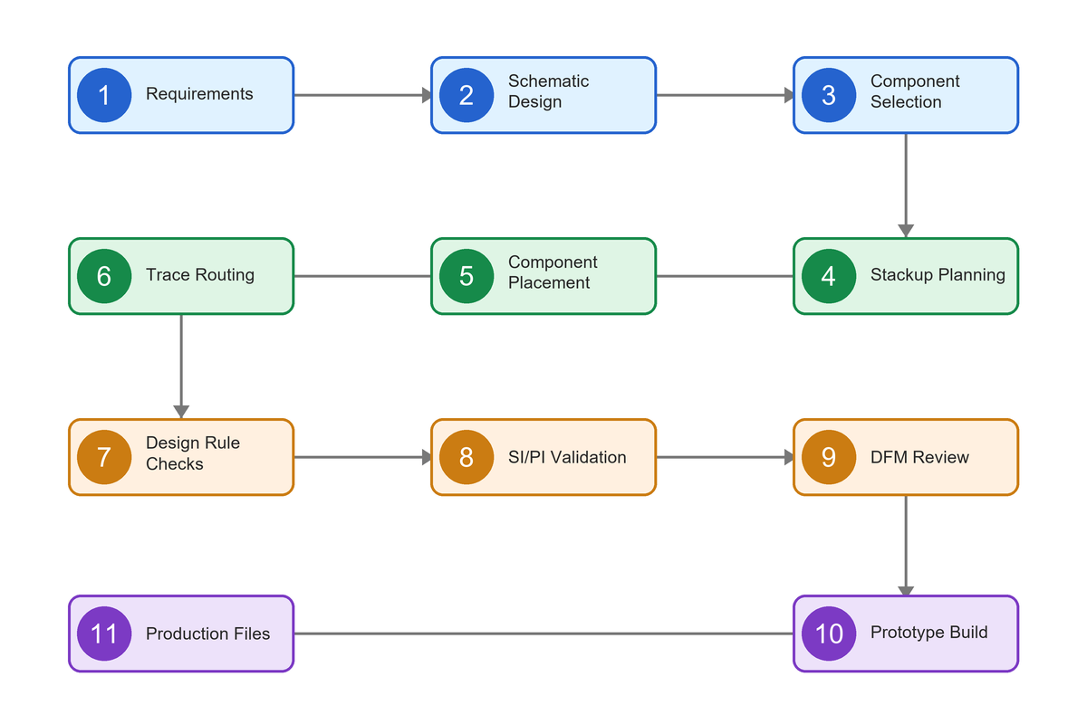
Step 1: Define Product and Electrical Requirements
Gather electrical, mechanical, and regulatory specifications. Define target cost parameters, board footprint, operating environments, and total production volumes.
Step 2: Create the Electronic Schematic
Draft logical circuit connections using specialized computer-aided design tools. Group components logically into functional blocks (power management, microcontroller, analog front-end, I/O interfaces) and assign net names to signal lines.
Step 3: Select and Validate Components
Choose active ICs and passive devices based on performance, package size, unit cost, lifecycle stage (avoiding End-of-Life parts), and active distributor inventory.
Step 4: Plan the PCB Stackup
Work with your manufacturing partner to define the layer stackup: copper weight (e.g., 1 oz or 2 oz), dielectric thickness, core materials, and target layer ordering to balance signal integrity and fabrication cost.
Step 5: Place Components on the PCB
Import schematic netlists into the layout editor. Execute physical placement according to functional signal flow, prioritizing high-speed lines, power conversion stages, physical connectors, and thermal dissipation paths.
Step 6: Route Traces and Critical Signals
Connect pads with copper traces. Route high-speed differential pairs, sensitive analog signals, and clock lines first, followed by general digital signal lines and heavy power copper pours.
Step 7: Perform Design Rule Checks
Run automated Design Rule Checks (DRC) inside your CAD tool to catch layout errors, including clearance violations, short circuits, dangling traces, and unrouted nets.
Step 8: Validate Signal, Power, and Thermal Performance
Perform computer simulations for PCB signal integrity, PCB power integrity, and thermal dissipation. Analyze signal eye diagrams, voltage drops (IR drop), and thermal hot spots before committing to hardware.
Step 9: Complete the DFM Review
Perform a thorough PCB manufacturability review alongside your manufacturing team to verify drill aspect ratios, annular rings, solder mask dams, and component spacing tolerances.
Step 10: Build and Test the PCB Prototype
Order an initial batch of prototype boards and populated assemblies. Conduct rigorous hardware bench testing, functional debug, and environmental evaluations.
Step 11: Release Production-Ready Manufacturing Files
Generate standardized fabrication packages containing Gerber or ODB++ files, drill files, BOMs, pick-and-place location files, and assembly drawings for factory handoff.
PCB Layout Design: Key Engineering Considerations
A successful physical layout balances signal quality, power delivery, and thermal relief. Adhering to solid engineering principles during the PCB layout design process prevents costly redesigns.
| Engineering Factor | Design Focus | Common Failures / Risks |
| Component Placement | Logical functional grouping, thermal separation, short signal paths | High cross-talk, mechanical interference, difficult manual assembly |
| Trace Width & Spacing | Current capacity, IPC-2221 standards, voltage isolation | Trace overheating, dielectric breakdown, unexpected copper shorts |
| Power & Ground Planes | Low-impedance power distribution, solid ground return loops | Voltage ripple, ground bounce, radiated EMI noise |
| Differential Pairs | Equal length matching, tight coupling, consistent impedance | Phase skew, signal degradation, mode conversion |
| Thermal Management | Thermal vias, copper pours, heatsink mounting pads | Component thermal throttling, solder joint stress, premature field failures |
| EMI & EMC | Ground loops, edge shielding, decoupling capacitor loops | Failing FCC/CE emissions, external noise vulnerability |
Component Placement and Circuit Organization
Group components by functional blocks. Keep high-frequency digital components separate from sensitive analog inputs. Position decoupling capacitors directly adjacent to power pins on integrated circuits to minimize trace inductance.
Trace Width, Spacing, and Routing
Calculate trace widths using IPC-2221 formulas based on expected current draw and allowed temperature rise. Maintain adequate trace-to-trace spacing to prevent dielectric breakdown and capacitive cross-talk.
Power and Ground Plane Design
Dedicate solid, uninterrupted copper layers to ground planes. Continuous ground planes provide low-impedance return paths for high-speed signals, reducing electromagnetic radiation and ground bounce. Avoid routing traces across splits in ground planes.
Differential Pairs and High-Speed Signals
Route high-speed differential signals (such as USB 3.0, HDMI, or Ethernet) with matched trace lengths and controlled trace gaps. Maintaining consistent differential impedance prevents signal reflection and jitter.
Thermal Management and Heat Dissipation
High-power components like MOSFETs, motor drivers, and fast processors require effective thermal distribution. Incorporate thermal vias placed directly under exposed ground pads to draw heat into internal ground planes or external heatsinks.
EMI and EMC Considerations
Minimize high-frequency loop areas. Place EMI filtering components (ferrite beads, TVS diodes, common mode chokes) as close as possible to connector entry points to keep noise from entering or leaving the enclosure.
Via, Drill, and Layer Stackup Requirements
Match via types (through-hole, blind, buried, microvia) to the board’s density and layer count. Ensure drill aspect ratios (board thickness divided by drill diameter) remain within standard manufacturing capabilities (typically less than 10:1 for through-holes).
Related: EMS Electronic Manufacturing Explained: From Design to Mass Production (2026)
PCB Design for Manufacturing (DFM)
Design for Manufacturing ensures that a board layout can be produced reliably, repeatedly, and cost-effectively on standard factory equipment.
| Fabrication Rules | Assembly Rules | Supply Chain Rules |
|---|---|---|
| Min trace width | Solder mask dams | Active component status |
| Min hole clearance | Component spacing | Alternate package footprints |
| Annular ring width | Fiducial markers | Standard pitch passive sizing |
| Copper edge clearance | Thermal pad relief | Readily available board laminates |
What Is PCB DFM?
PCB DFM combines fabrication rules (Design for Fabrication) and assembly rules (Design for Assembly). It aligns circuit geometry with real-world machinery capabilities, such as chemical etching limits, optical registration tolerances, pick-and-place nozzles, and automated soldering equipment.
Why DFM Should Start During PCB Design
Applying DFM for PCB design during early layout prevents costly manufacturing delays. Discovering an insufficient annular ring or an un-solderable pad pattern during factory pre-production checks stops line setups, while finding it after production causes scrap runs.
PCB Fabrication Design Considerations
- Maintain minimum trace width and space tolerances allowed by your fabricator.
- Ensure adequate copper-to-edge clearances to prevent exposed copper during board profiling.
- Size annular rings correctly to absorb drill registration drift.
PCB Assembly Design Considerations
- Provide consistent component pad sizes to prevent “tombstoning” during surface-mount reflow.
- Maintain adequate component clearance to allow pick-and-place nozzle access and optical inspection.
- Include standardized fiducial marks on panel corners and fine-pitch IC footprints for camera registration.
Component Availability and Supply Chain Considerations
Designing with rare or single-sourced parts introduces severe lead-time risks. Validate distributor stock levels early and design alternate pin-compatible footprints on the board whenever possible.
Design Tolerances and Manufacturing Capabilities
Standard commercial PCB fabrication utilizes 4/4 mil (0.1 mm) trace width/spacing and 0.2 mm minimum drill diameters. Exceeding these limits into ultra-fine feature territory requires advanced HDI processes, which increases board costs.
PCB Panelization and Production Efficiency
Arrange individual PCBs into standard manufacturing panels (e.g., 18×24 inches). Include breakaway tabs or V-score lines, tooling holes for assembly fixtures, and edge rails for SMT conveyor belts.
How PCB Design Affects Manufacturing Cost
Engineering decisions directly drive unit costs. Understanding how physical choices scale helps balance performance targets with project budgets.
Number of PCB Layers
Layer count is the largest single cost driver in fabrication. Moving from a 2-layer board to a 4-layer board increases raw board costs by approximately 30% to 50%, while adding extra layers adds laminating steps and processing time.
Board Size and Material Selection
Larger board areas require more copper-clad laminate material. Choosing specialized high-frequency laminates (like Rogers) or high-TG materials for elevated heat environments increases raw material costs compared to standard FR-4.
Component Selection and Availability
Fine-pitch BGA packages or small passive packages (0201 or 01005) increase SMT placement time and demand precise, high-cost assembly equipment. Standardizing on common, readily available components reduces unit purchase prices and setup fees.
Manufacturing Tolerances and Advanced Features
Specifying ultra-tight tolerances, microvias, blind/buried vias, gold surface finishes (ENIG), or heavy copper weights adds specialized processing steps at the factory.
PCB Assembly Complexity
Double-sided SMT assembly requires two separate reflow soldering cycles. Adding through-hole components introduces manual insertion steps or wave soldering setups, driving up labor costs.
Testing and Inspection Requirements
Demanding 100% In-Circuit Testing (ICT), custom functional test fixtures, or extensive X-ray inspection adds labor and tooling costs, but safeguards against field failures in mission-critical applications.
Production Volume and Manufacturing Scale
Fixed setup costs—such as stencil fabrication, SMT programming, and ICT test fixture manufacturing—are amortized over total batch sizes. Moving from prototype volumes (10–50 units) to mass production (10,000+ units) significantly lowers per-unit costs.
PCB Prototyping and Design Validation
Prototyping forms the crucial bridge between initial engineering models and volume manufacturing.
Why PCB Prototypes Are Important
Prototypes validate electrical schematics, physical dimensions, software firmware integration, and thermal performance in real-world environments before committing capital to mass production tooling.
Prototype PCB Fabrication and Assembly
Low-volume prototype builds prioritize fast turnarounds over scale pricing. Quick-turn fabrication plants produce raw boards in 24 to 72 hours, enabling hardware engineers to begin rapid bench testing.
Functional and Electrical Testing
Once assembled, prototype boards undergo power-rail checks, signal continuity checks, communication protocol verification, and full system functional testing.
Identifying and Correcting Design Issues
Early testing uncovers unexpected bugs—such as reversed pinouts, noisy voltage regulators, or mechanical interference with enclosure walls. Fixing these issues on initial prototypes avoids expensive scrap during volume runs.
Moving From Prototype to Production
After functional validation, engineers freeze the board layout, update manufacturing documentation, incorporate minor DFM refinements, and prepare for production testing validation steps.
Related: Drop Forging: Process, Types, Materials, Benefits, Applications & Cost Guide
PCB Testing and Quality Control
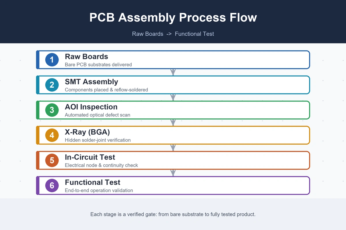
Rigorous testing guarantees that every assembled board leaving the factory meets mechanical, electrical, and quality specifications.
Electrical and Functional Testing
Bare-board flying probe tests verify that unpopulated PCBs have no open circuits or hidden electrical shorts before component loading.
Automated Optical Inspection (AOI)
High-resolution camera systems inspect populated boards immediately after SMT reflow. AOI checks for missing components, misaligned pins, solder bridges, and lifted leads.
X-Ray Inspection for PCB Assembly
Ball Grid Array (BGA) chips and bottom-terminated QFN packages have hidden solder joints underneath their bodies. Automated X-ray inspection inspects hidden solder voids and shorts beneath IC packages.
In-Circuit Testing (ICT)
ICT uses a “bed of nails” test fixture to press against specific test points on the board, checking individual passive values, diode orientations, and IC pin connections in seconds.
Reliability and Environmental Testing
Mission-critical products undergo environmental stress testing, including thermal cycling, vibration testing, and burn-in testing to catch latent infant mortality defects.
Traceability and Quality Documentation
Assigning unique serial numbers and 2D matrix barcodes to boards tracks component lot numbers, machine assembly lines, and inspection records across the full product lifecycle.
From PCB Prototype to Mass Production
Scaling up hardware manufacturing follows an industry-standard validation methodology that ensures high yields and consistent quality.
| Stage | Typical Quantity | Primary Objective |
|---|---|---|
| EVT (Engineering) | 10 – 50 units | Validate core electrical performance |
| DVT (Design) | 50 – 200 units | Verify mechanical & regulatory compliance |
| PVT (Production) | 200 – 1,000+ units | Test mass production tooling & yield |
| Mass Production (NPI) | Full volume | Continuous output, optimized cost |
Engineering Validation Test (EVT)
EVT builds confirm that the core electronic design works. Engineers build 10 to 50 prototype units to verify functional performance, run power rail checks, and correct major design flaws.
Design Validation Test (DVT)
DVT builds test the fully integrated product inside its final enclosure. Units undergo environmental testing, drop testing, and official regulatory compliance certifications (FCC, CE, UL).
Production Validation Test (PVT)
PVT runs test the mass production line itself. Built using final factory tooling, assembly line operators, and automated test fixtures, PVT validates line speed, manufacturing yield, and cycle times.
NPI and Production Readiness
New Product Introduction (NPI) managers coordinate the transfer of validated designs, assembly instructions, component supply chains, and test procedures to high-volume manufacturing lines.
Scaling PCB Assembly for Mass Production
Once PVT yields exceed target benchmarks (typically >98%), the factory ramps up mass production, shifting focus to supply chain optimization, component buffer management, and continuous process controls.
PCB Manufacturing and Assembly Process
Modern surface mount assembly relies on high-speed automated equipment capable of placing tens of thousands of components per hour.
PCB Fabrication
Raw manufacturing begins by laminating glass-epoxy sheets, photo-imaging circuit traces, etching excess copper, drilling vias, plating copper through-holes, applying solder mask layers, and printing silkscreen labels.
Component Sourcing and Procurement
Procurement teams source raw parts from franchised distributors and component manufacturers according to the approved BOM, storing moisture-sensitive devices in climate-controlled environments.
SMT and Through-Hole Assembly
- Surface Mount Technology (SMT): Automated machines print solder paste through stainless steel stencils onto pads, place SMD components with vacuum nozzles, and pass boards through multi-zone reflow ovens.
- Through-Hole Assembly: Large components, heavy connectors, and power transformers are inserted manually or with selective soldering machines, followed by wave soldering.
PCB Programming and Firmware Loading
Automated programming stations flash bootloaders, operating systems, and functional microcode onto microcontrollers and flash memory chips prior to final testing.
Functional Testing and Inspection
Custom functional test rigs simulate real-world operating inputs and measure outputs, ensuring every board meets functional specifications before enclosure installation.
Final Assembly and Production Quality Control
Tested circuit boards are installed into final enclosures, wired to battery assemblies or displays, packaged in retail boxes, and subjected to final Out-of-Box Audits (OBA).
PCB Manufacturing Files and Documentation
Clear, standardized manufacturing documentation prevents factory misinterpretations and ensures smooth handoffs to your production partner.
Gerber Files
Gerber files (RS-274X or Gerber X2) are vector images that describe every physical layer of the board: copper layers, solder mask openings, silkscreen text, and paste layers.
Drill Files
Excellon drill files specify exact X-Y coordinates, hole sizes, and plating requirements (plated vs. non-plated through-holes) for every hole drilled into the board.
Bill of Materials (BOM)
A production-ready BOM includes manufacturer part numbers, component descriptions, package types, reference designators (e.g., R1, C5, U2), and approved alternate parts.
Pick-and-Place Files
Also known as Centroid files, these text files list the X-Y coordinates, rotation angles, board side (top/bottom), and reference designators for automated SMT placement equipment.
Assembly Drawings and Manufacturing Drawings
Assembly drawings detail mechanical dimensions, component height restrictions, panelization breakaway notes, special potting instructions, and critical inspection points.
PCB Specifications and Test Requirements
Documentation detailing IPC class standards (IPC-A-610 Class 2 or Class 3), surface finish specifications, solder mask color, test point coverage, and functional pass/fail parameters.
Related: Compression Molding: Process, Materials, Types, Benefits, Applications & Cost Guide
Common PCB Design Problems That Cause Manufacturing Issues
Avoiding common layout oversights saves production cycles and prevents yield drops on the assembly line.
| Problem | Practical Prevention |
|---|---|
| Incorrect Footprints | Verify CAD symbols against physical part datasheets. |
| Inadequate Clearance | Set CAD clearance constraints according to fabricator. |
| Poor Component Placement | Keep SMT passives balanced; align polarized components. |
| Neglecting Thermal Paths | Place thermal vias directly beneath power pads. |
| Missing Test Points | Add accessible 1.0 mm pads on all critical nets. |
Designing Without Manufacturing Constraints
Ignoring fabricator capabilities leads to un-routable designs, drill breaks, copper shorts, or impossible assembly requirements.
Incorrect Component Footprints
Mismatched pin pitches, reversed pin numbering, or undersized pads prevent components from fitting or soldering correctly on the line.
Insufficient Clearance and Trace Spacing
Tightly packed copper traces placed without adequate clearance risk solder bridging during assembly or electrical shorting in high-humidity field environments.
Poor Component Placement
Placing heavy components near board edges or clustering high-profile parts next to small passives blocks pick-and-place heads and impedes automated optical inspection camera angles.
Inadequate Thermal Management
Failing to add thermal relief spokes to copper plane connections makes soldering component pads difficult, causing uneven heating and cold solder joints.
Ignoring Component Availability
Selecting obscure components without checking market stock levels can stall an entire production run if parts become unavailable mid-build.
Missing Test Points and Test Requirements
Omitting accessible 1 mm test pads on crucial power, programming, and signal nets prevents automated ICT fixtures from verifying board health during assembly.
Incomplete or Incorrect Manufacturing Documentation
Mismatched BOM part numbers, missing drill tables, or outdated Gerber revisions lead to incorrect factory setups and scrapped production batches.
How to Choose a PCB Design and Manufacturing Partner
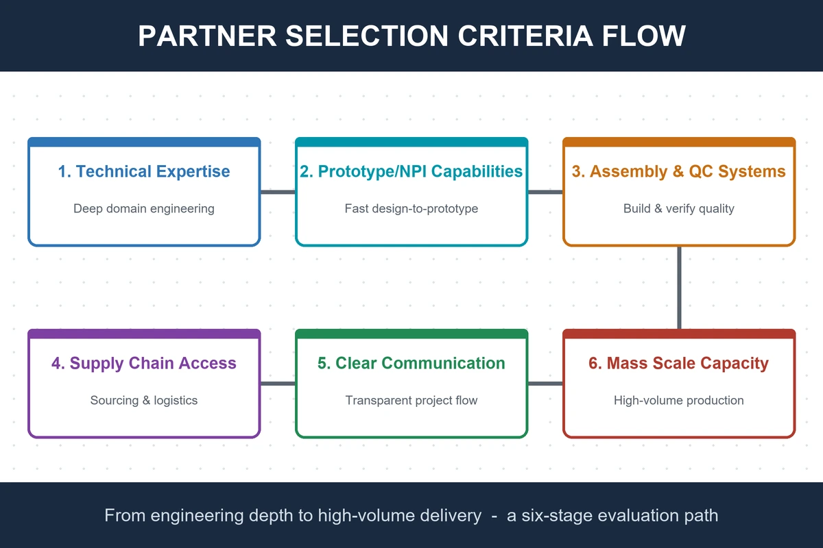
Selecting an experienced electronics partner determines how smoothly your hardware project transitions from design drawings to physical products.
Evaluate Engineering and PCB Design Expertise
Look for manufacturing partners with in-house hardware engineering teams who understand advanced signal routing, power planes, thermal management, and DFM rules.
Check Prototype and NPI Capabilities
Verify that your partner offers dedicated quick-turn prototyping and structured NPI processes to handle EVT, DVT, and PVT engineering builds smoothly.
Assess PCB Assembly and Testing Capabilities
Ensure the factory operates automated SMT placement equipment, 3D AOI, X-ray inspection, and flexible functional testing systems tailored to your technical requirements.
Verify Component Sourcing and Supply Chain Support
Choose partners with strong relationships with authorized global component distributors, enabling them to secure genuine parts, manage buffer stocks, and resolve component shortages.
Review Quality Management and Production Controls
Confirm essential industry certifications—such as ISO 9001, ISO 13485 (medical), or IATF 16949 (automotive)—which demonstrate rigorous quality tracking protocols.
Evaluate Communication and Project Management
Working with engineering teams who provide clear design feedback, detailed DFM reports, and responsive project management reduces project risk.
Confirm Mass Production Capacity
Ensure your partner can scale seamlessly from initial hundred-unit prototype runs to tens of thousands of units per month without needing to re-qualify new assembly plants.
When Should You Work With an OEM or ODM PCB Manufacturing Partner?
Different hardware development models require different partner support levels.
| OEM Model (Original Equipment) | ODM Model (Original Design) |
|---|---|
| You provide complete design files | You provide product idea & feature specs |
| Partner executes DFM & production | Partner handles engineering design & hardware |
| Retain full proprietary IP | Turnkey development from concept to box build |
When You Have an Existing PCB Design
If your in-house team has already created schematic and layout files, an OEM manufacturing partner reviews your files for DFM, handles raw fabrication, sources parts, and executes SMT assembly.
When You Need PCB Design and Product Development
If you have a clear product concept but lack in-house hardware engineering bandwidth, an ODM partner provides end-to-end design, schematic drafting, layout, prototyping, and volume production services.
When You Need Prototype-to-Mass-Production Support
Working with an integrated partner avoids handoff friction between separate design houses and contract assembly factories, ensuring that prototype learnings carry directly into volume production.
When You Need Component Sourcing and Supply Chain Management
Partners with established procurement networks mitigate component obsolescence risks, negotiate volume pricing, and keep production lines running smoothly.
When You Need an End-to-End Electronics Manufacturing Partner
An end-to-end partner manages raw board fabrication, SMT assembly, firmware loading, custom enclosure injection molding, final box-build packaging, and functional testing under a single roof.
PCB Design Services for OEM & ODM Product Development
Partnering with an experienced turnkey hardware specialist streamlines every stage of hardware creation.
Custom PCB Design and Layout
Professional layout engineering converts functional concepts into optimized, multi-layer circuit board layouts tailored to your exact mechanical footprint and performance criteria.
Hardware Engineering and Product Development
Complete hardware design capabilities include system architecture planning, power management optimization, wireless system integration, and regulatory compliance planning.
PCB Prototyping and Validation
Rapid engineering prototyping allows you to test physical hardware iterations, refine firmware drivers, and validate mechanical fit before launching full-scale production runs.
DFM and Design Optimization
Thorough pre-production DFM audits identify hidden layout errors, refine pad geometries, balance copper planes, and optimize assembly yields before committing to volume manufacturing tooling.
PCB Assembly and Testing
State-of-the-art surface-mount and through-hole assembly lines backed by AOI, X-ray inspection, and custom functional test fixtures guarantee high assembly quality.
NPI and Mass Production
Structured NPI processes guide your hardware through EVT, DVT, and PVT stages, ensuring smooth scaling into high-volume manufacturing with minimal yield drop.
End-to-End OEM/ODM Manufacturing Support
From concept sketching and PCB layout to final plastic enclosure tooling, system assembly, and shipping, turnkey services streamline product development under one accountable partner.
From PCB design and prototyping to full-scale OEM and ODM manufacturing, Precintl helps turn your electronic product concept into reliable, market-ready hardware.
Why Choose Precintl for PCB Design and Manufacturing?
At Precintl , we deliver reliable, end-to-end ODM, OEM, and custom electronics design solutions tailored to your operational requirements.
Engineering Expertise From Design to Production
Our senior engineering team brings decades of combined experience in high-speed digital layout, power electronics, RF design, and thermal engineering. We turn complex technical challenges into manufacturable hardware products.
Integrated PCB Design, DFM, Prototyping, and Assembly
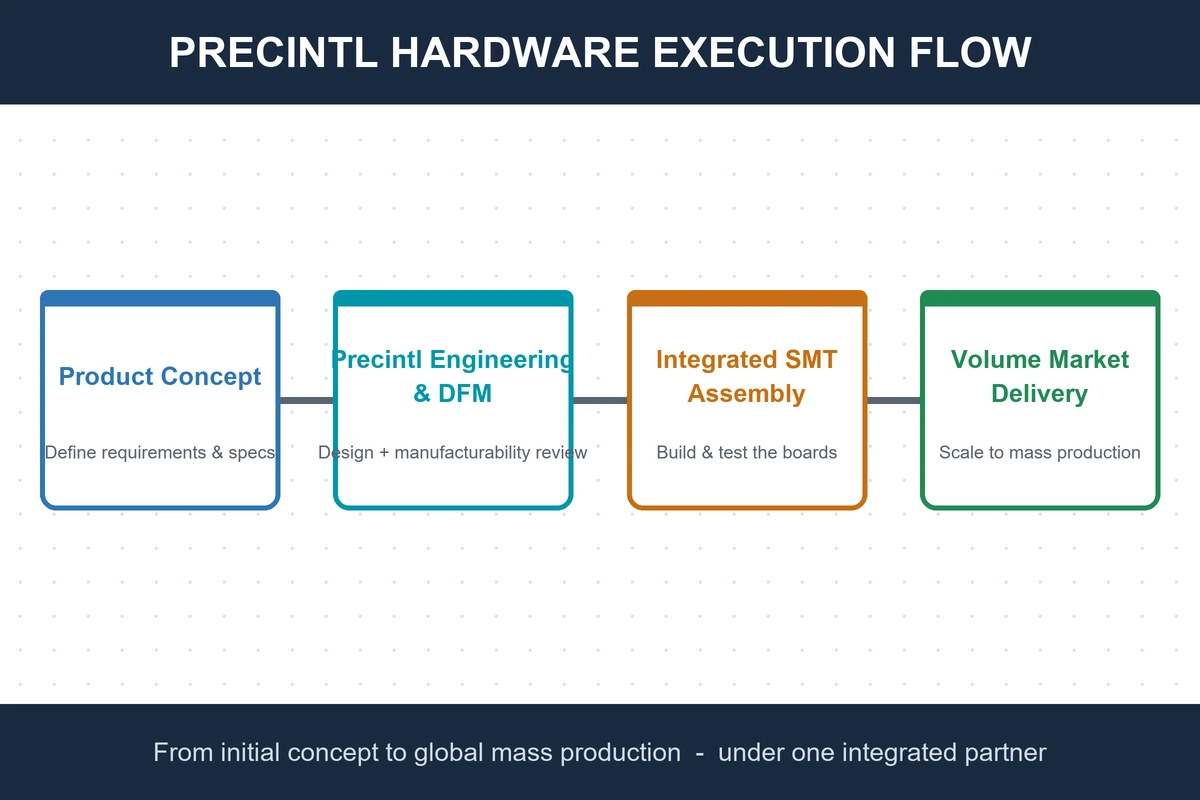
We unite layout design, DFM analysis, quick-turn prototyping, component procurement, and volume SMT assembly under a single operational umbrella. This integration eliminates handoff errors and speeds up market entry.
Component Sourcing and Supply Chain Support
Through established relationships with authorized global component distributors, we source genuine parts, identify cost-effective alternates, and manage supply chain buffers to keep lines running without interruption.
EVT, DVT, PVT, and NPI Experience
Our structured NPI methodology ensures your product passes through EVT functional checks, DVT compliance testing, and PVT line yield validation steps before starting full-scale production.
Quality Control and Production Testing
Every board produced at Precintl undergoes rigorous quality checks—including bare-board flying probe tests, 3D AOI, X-ray inspection, and custom functional testing—ensuring field-ready reliability.
Prototype-to-Mass-Production Capability
Whether you need 10 prototype units for bench testing or 100,000 units for global distribution, our flexible manufacturing infrastructure scales smoothly alongside your business growth.
One Manufacturing Partner for the Complete Product Lifecycle
Precintl supports your product through its entire lifecycle—from initial schematic design and mechanical enclosure fitting to mass assembly, firmware loading, and box-build packaging.
PCB Design FAQs
What is PCB design and why is it important?
PCB design is the process of mapping electronic schematics onto physical circuit board layouts. It defines how traces route signals, how power planes distribute current, and where components sit on a substrate. Good design ensures electrical functionality, prevents thermal issues, and enables efficient automated assembly.
How long does PCB design take?
Design timelines depend on board complexity. Simple 2-layer boards can take 3 to 7 days, while complex 8-to-12-layer HDI or high-speed boards require 3 to 6 weeks for schematic drafting, component placement, trace routing, and DFM reviews.
How much does PCB design cost?
Design costs vary based on component count, layer count, signal speeds, and required certifications. Basic layouts start around a few hundred dollars, whereas high-density, multi-layer commercial designs involving custom hardware development range from several thousand to tens of thousands of dollars.
What files are required to manufacture a PCB?
To manufacture a raw PCB and assemble components, factories require:
- Gerber files (or ODB++)
- Excellon drill files
- Bill of Materials (BOM) with manufacturer part numbers
- Pick-and-Place (Centroid) files
- Assembly and mechanical drawings
Can an OEM/ODM manufacturer handle PCB design, assembly, and mass production?
Yes. An integrated OEM/ODM partner like Precintl handles the complete lifecycle—including initial circuit schematic design, PCB layout design, DFM optimization, prototype fabrication, SMT assembly, functional testing, and full mass production.